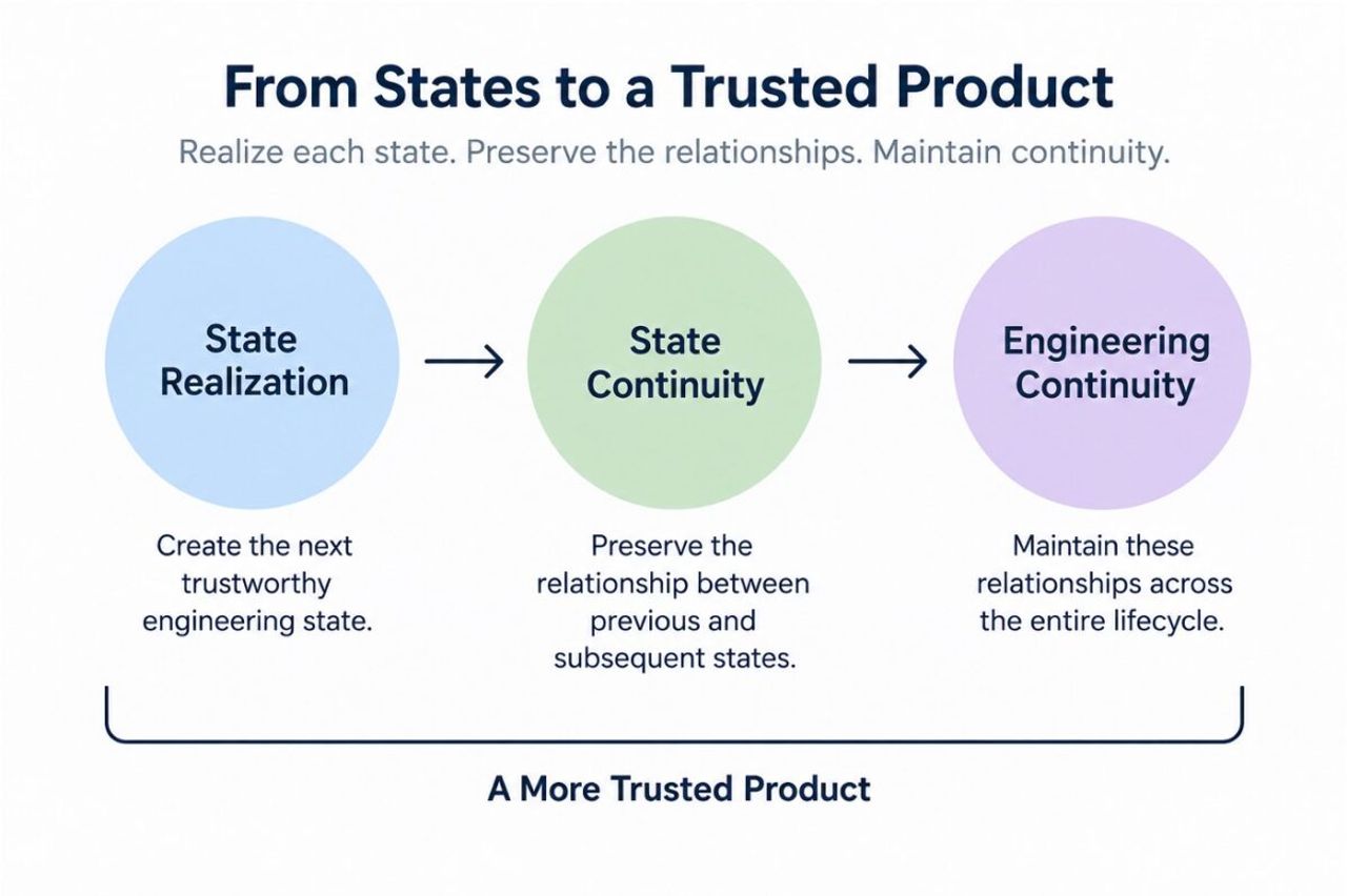
The core argument is deceptively simple: chip development is treated as a relay race through architecture, design, fabrication, packaging, and qualification, when what actually determines product success is preserving the relationships between those stages from original intent through lifecycle learning. Most organizations advance the state but drop the connective tissue.
Globally, this problem is compounding faster than tooling can absorb. The shift to chiplets and heterogeneous integration means a single product now threads through multiple EDA vendors, foundries, and OSAT partners, each with its own data model and its own idea of 'done.' Every handoff is a place where design intent, test conditions, and failure history get flattened into a spec sheet and a GDS file. When a part misbehaves at qualification or in the field, teams cannot cheaply trace back to the decision that caused it, so they re-derive knowledge they already paid for. The economic signature of this is rising verification cost, more silicon respins, and slower time-to-yield precisely as demand for AI accelerators makes every lost week expensive. It is a data-architecture problem masquerading as an engineering-discipline problem.
The uncomfortable truth is that most of the industry's investment has gone into reaching the next state faster, not into making states legible to each other. Continuity is unglamorous infrastructure, so it stays underfunded until a costly field failure forces a reckoning.
For Japan, this lands at an awkward moment. The country is rebuilding advanced-node capability and leaning on its dominance in materials and equipment, where firms like Tokyo Electron and Shin-Etsu sit upstream of exactly the handoffs this problem describes. A fab revival built on world-class hardware but fragmented, per-tool data trails will import the state-continuity gap by default. Japanese manufacturers have deep MES and quality-traceability culture on the production floor, yet that rigor rarely extends backward into design intent, leaving a seam between how a chip was meant to work and how it is actually built and screened.
For Japanese SIers and enterprise IT teams, this is a genuine opening rather than a threat. The valuable work is no longer bespoke EDA scripting; it is building the connective data layer, the PLM integration, traceability schema, and cross-vendor lineage that let intent survive every handoff. RPA and workflow automation that simply move files between silos will make the problem worse by industrializing lossy handoffs. The teams that win will treat state continuity as the product, positioning themselves as the integrators who make Japan's manufacturing precision legible end to end rather than just faster in each isolated step.




