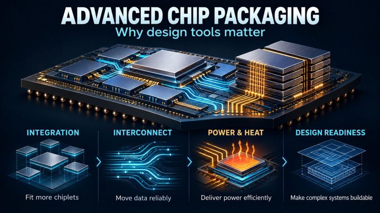
The interesting signal here is where the difficulty is migrating. For a decade the industry framed semiconductor progress as a manufacturing race, measured in nanometers and yield. That story is now incomplete. As systems pack logic dies, memory stacks, power delivery, and increasingly optical I/O into a single package, the hard part is no longer building each component but making them behave as one coherent system. TSMC's framing of inter-die complexity for 3D multi-die designs confirms what many architects have suspected: packaging has become a design discipline, and the design tools were never built for it.
The global implication is a quiet reshuffling of who holds leverage. Foundry capacity remains a chokepoint, but the new scarce resource is the ability to co-optimize across dies, thermals, power, and interconnect before anything is taped out. This favors players who own both the physical packaging IP and the design methodology, and it pulls EDA vendors, foundries, and hyperscaler chip teams into tighter coupling. It also raises the cost of entry. A startup can rent leading-edge wafers, but it cannot easily rent the multi-year discipline of getting a heterogeneous package to close timing, power, and heat simultaneously. Expect the performance gap between well-resourced integrated design teams and everyone else to widen, not narrow.
There is a second-order risk worth naming. As more system value moves into the package, a single co-design error becomes far more expensive than a masking defect, because it invalidates an entire integrated assembly rather than one die. This changes risk models for anyone building custom silicon, and it rewards conservative, methodology-heavy engineering cultures over move-fast experimentation.
For Japan, this shift plays to genuine structural strengths and exposes a familiar gap. On the strength side, Japan sits deep in the packaging supply chain: materials, substrates, precision equipment, and testing are areas where Japanese suppliers hold real, defensible positions. If the industry's center of gravity moves toward packaging and integration, that is a tailwind for the domestic materials and equipment base, and it strengthens the strategic logic behind the recent push to rebuild advanced manufacturing capacity on Japanese soil.
The gap is on the design and methodology side. Japanese enterprises and their SIer partners are strong at manufacturing execution but historically thinner in the frontier chip-design and system co-optimization layer where value is now concentrating. For domestic firms pursuing custom silicon, whether for automotive, industrial systems, or edge AI, the practical lesson is that in-house design methodology and cross-domain engineering talent matter more than access to a foundry slot. SIers and development teams supporting hardware-adjacent clients should treat packaging-aware design, thermal and power modeling, and heterogeneous integration as capabilities to build now rather than outsource later. The companies that pair Japan's materials advantage with credible in-house design discipline will be the ones that capture the upside of this transition instead of merely supplying it.




