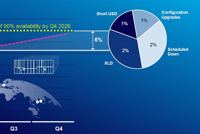
ASML confirmed at SEMICON Taiwan that its High NA EUV platform has now been used to build a high-volume logic product, the point where 0.55 NA moves from qualification into live production service.
The strategic weight here is not the machine, it is the timeline compression it implies. High NA lets fabs pattern the tightest features in a single exposure rather than stitching multiple masks together. Fewer process steps means fewer defect opportunities and faster cycle times, which matters enormously when the leading logic nodes are the bottleneck for AI accelerators. Whoever qualifies High NA first at yield gets a structural cost-and-density advantage that compounds across every generation of GPU and custom silicon. That is why this milestone reads less like a lab result and more like a starting gun for the next capex cycle among the three companies that can actually afford these tools.
The flip side is concentration risk. Each High NA system carries a nine-figure price tag and ASML remains the sole supplier, so a single vendor's shipment cadence now gates the entire frontier of computing. For hyperscalers and chip designers, this narrows sourcing options precisely as demand for advanced logic is exploding. Expect longer forward commitments, tighter allocation politics, and renewed government interest in who gets tool access and when.
For Japan, this is a quieter but real opportunity rather than a threat. ASML sits at the center, but a High NA node is only as good as the ecosystem around it, and much of that ecosystem is Japanese. Advanced photoresists, blank masks, deposition and etch equipment, and metrology all lean heavily on Japanese suppliers whose content per wafer tends to rise, not fall, as patterning complexity increases. A production High NA node expands the addressable market for these firms even though none of them build the scanner.
The sharper question is for Japan's own leading-edge ambitions. A domestic 2nm effort has publicly tied its roadmap to advanced EUV, and ASML's production milestone sets an external benchmark that Japanese fabs will be measured against. The practical takeaway for Japanese enterprises, SIers, and their clients is downstream: the compute that will run next-generation AI workloads is being defined now at the lithography layer. Procurement teams planning multi-year AI infrastructure should treat advanced-node availability, not model licensing, as the harder constraint, and factor tool-supply concentration into capacity and cost forecasts rather than assuming linear price declines.




