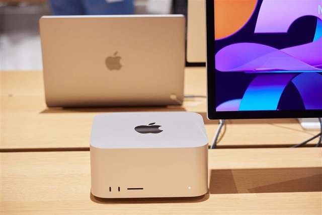
Apple's latest Mac mini and Mac Studio quietly break an industry convention that has held for a decade: that the newest process node belongs in the most powerful product. Here the 2nm M6 debuts in the cheapest box, while the flagship M5 Ultra remains on 3nm, stitching four dies together via advanced packaging. This is not a mistake—it is a signal about where leading-edge performance now comes from.
The strategic message for global executives is that transistor density is no longer the sole lever of chip strength. As node shrinks deliver diminishing returns and each new generation costs dramatically more per wafer, the marginal gain from 3nm to 2nm has narrowed. Apple is instead extracting performance from architecture and packaging—die-to-die interconnect bandwidth, memory proximity, and multi-die integration. The M5 Ultra's four-die design shows that assembling silicon well now matters as much as printing it finer. That reframes the competitive battlefield: TSMC's advanced packaging capacity (CoWoS, SoIC-class technologies) becomes as strategically scarce as the 2nm line itself, and the bottleneck for high-end compute shifts from lithography to assembly.
This also lets Apple manage cost and yield pragmatically. Early 2nm yields are low and volumes constrained, so seeding the node in a high-volume, lower-margin entry product is a clever way to ramp learning while reserving mature 3nm for premium SKUs where reliability and margin matter most. Expect the same playbook—new node in volume products, packaging in flagships—to spread across the datacenter accelerator market, where Dell's raised AI-server outlook underscores that demand is chasing integration, not just node numbers.
For Japan, the implications run deeper than most realize. The pivot toward advanced packaging plays directly to Japanese strengths: firms supplying photoresists, packaging substrates, bonding equipment, and precision materials sit upstream of exactly the CoWoS-style processes now defining chip strength. As Japan courts fabs and packaging investment through its domestic semiconductor revival, the message is that the value is migrating from raw front-end lithography toward back-end integration—an area where Japanese materials and tooling players hold durable positions.
For Japanese enterprises and SIers, the near-term takeaway is procurement literacy. As Apple silicon and similarly packaged chips make workstation-class local compute cheaper, on-device AI inference for design, engineering, and creative teams becomes viable without cloud dependence. SIers building client infrastructure should stop equating 'newest node' with 'best value' and instead assess real workload performance. The decoupling of process from power means spec sheets lie more than ever—benchmarks, not nanometers, should drive hardware refresh decisions for local development and edge-AI deployments.




