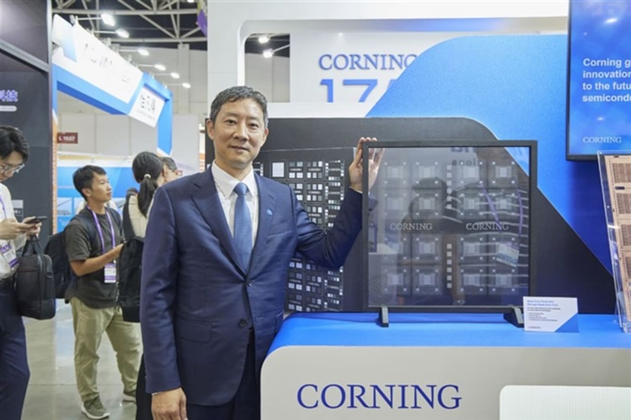
The center of gravity in semiconductors is moving off the wafer. With transistor scaling delivering diminishing returns, the binding constraint on AI performance is now how you feed data between chips, memory stacks, and racks. That reframes advanced packaging, co-packaged optics (CPO), glass core substrates, and panel-level fan-out from niche back-end steps into strategic control points. When a glassmaker starts describing itself as a semiconductor supply-chain player, it signals that materials science, not just lithography, decides who wins the next cycle.
The global logic is straightforward. AI clusters live and die on interconnect bandwidth and power efficiency. CPO moves the optical engine next to the switch or accelerator, cutting the energy tax of shuttling signals over copper. Glass core substrates promise flatter, larger, more electrically stable interposers than today's organic laminates, which matters as package sizes balloon past reticle limits. Both trends favor firms with deep expertise in glass formulation, optical fiber, and precision panel handling, and both widen the moat around whoever controls the material stack. The risk is concentration: a handful of specialized suppliers gate the entire AI hardware roadmap, and any yield stumble ripples straight into GPU availability.
For Japan this is closer to home advantage than to disruption. The country already anchors the high-end substrate and materials layer that this shift amplifies. Ibiden and Shinko Electric are entrenched in premium IC substrates, while AGC and Nippon Electric Glass bring exactly the glass-processing depth that a glass-core future demands. Photoresist, bonding, and inspection strengths across the domestic supplier base extend that position. The strategic question is whether Japanese firms move up from selling materials and components to owning integrated packaging platforms, or remain upstream price-takers as US and Taiwanese players capture the system-level margin.
For Japanese chipmakers, OSAT partners, and the equipment ecosystem, the practical implication is to treat packaging R&D as a core competitive investment rather than a cost line. Rapidus and the broader domestic revival effort will only pay off if leading-edge logic is matched by leading-edge assembly and optics onshore. Enterprises and SIers building AI infrastructure should also read this as a supply-signal: procurement lead times for accelerators will increasingly hinge on packaging and CPO capacity, not fab wafer starts, and capacity planning needs to reflect that new bottleneck.




