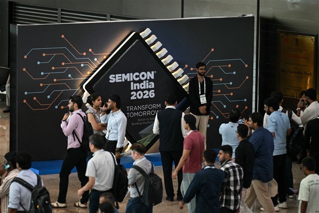
The signal from Semicon India 2026 is not the absence of a fab announcement but the deliberate substitution of one. Applied Materials, Lam Research, Micron, ASML, and Infineon chose the layers of the value chain that generate revenue without waiting on a customer's wafer starts—equipment, silicon components, assembly and test, research parks, design centers. That is rational capital discipline. A leading-edge fab is a multi-year, multi-billion-dollar bet against uncertain local demand and a thin talent base. The supporting ecosystem, by contrast, monetizes immediately, scales with global order books, and builds the workforce a future fab would need. India's Semicon 2.0 framework understood this sequencing; the multinationals simply validated it with checks.
The global implication is a maturing of the 'chip sovereignty' narrative. The reflex to equate national capability with front-end fabrication is giving way to a portfolio view, where materials, packaging, and design carry durable strategic weight and better returns. Advanced packaging in particular is where performance gains and margin increasingly concentrate. Expect more governments to court the mid-stream rather than chase a marquee fab that may sit underutilized. The risk for India is that a supporting industry without an anchor fab remains an export-processing node rather than a demand center—useful, but capturing less of the value it enables.
For Japan, this is both opening and pressure. Japan's structural strength sits precisely in the layers India is now building out: photoresists, silicon wafers, specialty chemicals, and process equipment. A funded Indian supporting industry expands the addressable market for Japanese materials and tool makers and offers a China-plus-one manufacturing footprint that many boards already want. But it also seeds future local substitutes, so the strategic play is to localize early—joint ventures, technical centers, and long-term supply agreements that lock in position before Indian capability matures.
For Japanese SIers and enterprise IT teams, the near-term action is in the design centers and research parks rather than the cleanroom. These sites need EDA integration, PLM systems, secure IP pipelines, and the engineering workforce infrastructure that surrounds chip design. That is billable, exportable work aligned with existing offshore relationships in India. SIers positioning as the systems and process layer for India's semiconductor buildout—not the silicon itself—can attach to a multi-year investment cycle without carrying fab-scale capital risk. The firms that treat India's chip ambition as a services and materials opportunity, rather than only a manufacturing headline, will read this moment correctly.




