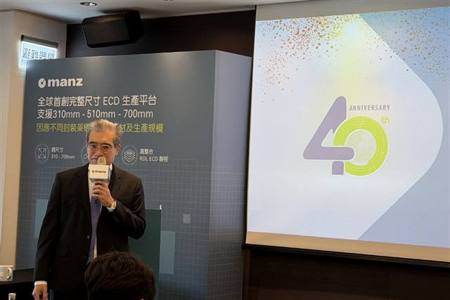
The economics of AI silicon are breaking the 300mm wafer. As accelerator dies balloon and chiplet integration multiplies, the circular wafer wastes too much area at the edges and caps how many large modules a substrate can yield. The industry's answer is the square panel—and it is now splitting into two distinct strategic tracks. FOPLP (fan-out panel-level packaging) is being positioned as the cost-reduction play for higher-volume, mainstream parts, while CoPoS (chip-on-panel-on-substrate) is being courted specifically by the AI-chip crowd that needs to stitch together massive compute-plus-HBM assemblies. Glass-core substrates sit further out on the roadmap as the eventual endgame.
The global takeaway is that packaging has become a genuine competitive battleground, not a back-end afterthought. Nvidia-class accelerators are already constrained less by transistor density than by advanced-packaging capacity—the CoWoS bottleneck of the past two years proved that. A move to panels changes the capital math entirely: different tools, different substrate suppliers, different yield-learning curves. Whoever masters panel warpage, die-shift, and fine-line redistribution at panel scale controls a chokepoint in the AI supply chain. This is why the same investor enthusiasm driving custom-inference bets—Etched's valuation doubling to a reported $21B in a month—will inevitably flow toward the packaging layer that makes such chips manufacturable at scale.
For Japan, this transition is unusually favorable, and it deserves more attention than it gets in Tokyo boardrooms. Japanese firms dominate precisely the inputs that panel-level packaging depends on: photosensitive dielectrics, ABF-class buildup materials, precision dispensing and lithography equipment, and the inspection tools needed to catch defects across a large panel where a single flaw scraps far more value than on a wafer. As the industry forks into FOPLP and CoPoS, demand for these materials and metrology systems compounds rather than commoditizes.
The risk for Japanese suppliers is strategic timing, not capability. FOPLP and CoPoS require different material formulations and tool specs; committing capacity to the wrong track, or hedging too cautiously across both, could cede first-mover advantage to Taiwanese and Korean packaging houses moving aggressively into panels. Japanese material vendors should be co-developing with OSATs now, not waiting for standards to settle.
For Japanese enterprise IT buyers and SIers, the second-order effect is what matters most: panel packaging is a lever to ease the AI-hardware supply crunch that—combined with reported memory price surges—is inflating every AI infrastructure budget. Firms planning on-prem AI clusters or GPU procurement over the next 24 months should treat packaging capacity as a leading indicator of accelerator availability and pricing, and build that volatility into their multi-year capex assumptions rather than assuming linear cost declines.




