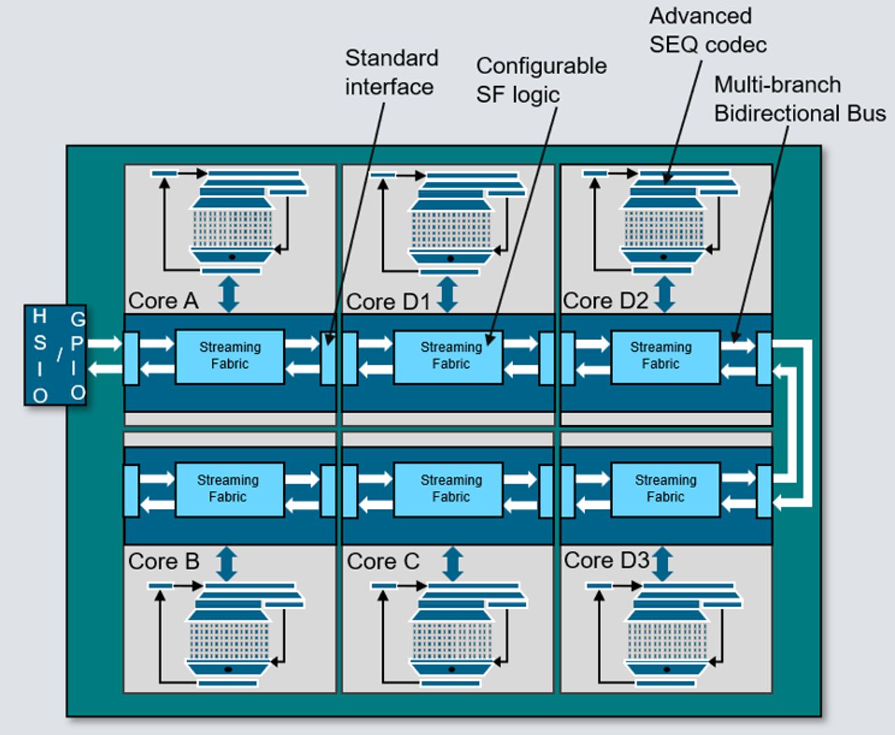
The underlying point is narrow but consequential: compression shrinks test data, yet moving that data efficiently across the chip is now an equal bottleneck for large AI and HPC devices.
The economics here are underappreciated at the executive level. Test is one of the few semiconductor cost lines that scales with complexity rather than benefiting from it. A frontier AI accelerator packs billions of transistors, wide multi-die assemblies, and dense on-chip fabrics, and each of those elements has to be exercised, isolated, and diagnosed. When test time per unit climbs, it eats directly into tester throughput, and automated test equipment is a capital-intensive, capacity-constrained resource. In a market where every high-end GPU and accelerator is already supply-limited, test throughput quietly becomes part of the ceiling on how many good die reach customers each quarter.
That is why the shift from raw compression toward hierarchical connectivity matters strategically. Getting compressed patterns to the right cores without saturating internal bandwidth determines whether design-for-test scales with chiplet and 3D-stacked architectures. As the industry moves to disaggregated dies and advanced packaging, test that once happened on a monolithic chip now spans multiple known-good-die checkpoints. Firms that treat DFT as an afterthought will pay in yield loss, longer ramps, and diagnostic blind spots precisely where margins on AI silicon are highest.
For Japan, this sits close to a genuine area of strength rather than a defensive story. Advantest anchors the global ATE market alongside a deep bench of Japanese suppliers in probe cards, handlers, and test sockets. Rising test complexity for AI and HPC parts expands the addressable value of that equipment base, but only if tooling keeps pace with hierarchical, multi-die test flows. The risk is that test scaling becomes software- and methodology-led, an area where Japanese hardware leaders have historically been less dominant.
For Japanese chip design teams and the fabless-adjacent players emerging around domestic AI and automotive silicon, the practical takeaway is to fund DFT and test architecture early in the design cycle, not at tape-out. SIers and EDA-adjacent service firms have a real opening here: test-methodology consulting, yield analytics, and diagnostic tooling for advanced packaging are higher-margin, defensible work than commodity implementation, and demand is being created by exactly the AI buildout everyone is chasing.




