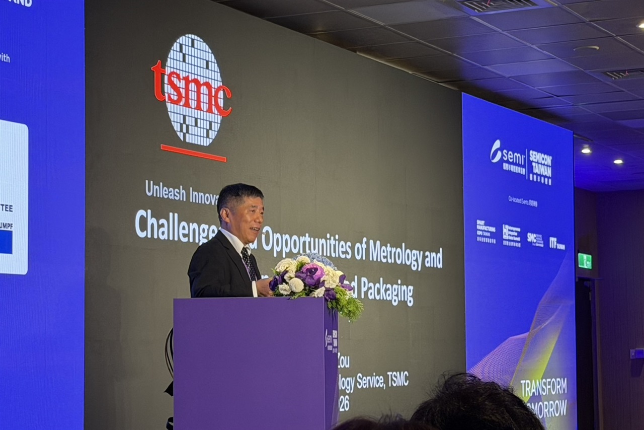
TSMC is pressing HBM and DRAM makers to design memory that X-ray tools can actually see through, because advanced packaging is burying defects deeper while the inspection process itself risks irradiating sensitive cells. Framed narrowly, this reads as a metrology footnote. It is not. It is a signal that the hardest problems in AI memory have migrated from the transistor to the stack.
The context matters. HBM is climbing vertically toward 12-high and 16-high configurations, moving toward hybrid bonding and ever-denser through-silicon vias. SK hynix's own framing at Hot Chips reinforces the point: future bandwidth gains depend less on DRAM circuit tricks and more on how cleanly you can integrate dozens of thin dies without voids, misalignment, or trapped defects. As the integrator behind CoWoS, TSMC sits downstream of that risk. A single flawed HBM stack can scrap an entire high-value accelerator package, so TSMC is effectively trying to enforce design-for-inspectability upstream, before defects become invisible and expensive.
The global implication is a shift in where value and bottlenecks sit. Yield economics for AI accelerators increasingly hinge on packaging test and inspection, not wafer fabrication alone. That raises the strategic weight of metrology, X-ray CT, acoustic imaging, and known-good-stack testing. It also creates a genuine engineering tension the industry rarely discusses openly: the same radiation used to find buried defects can corrupt the memory it inspects. Whoever solves inspection without compromising reliability gains leverage over the entire HBM supply chain.
For Japan, this is a rare tailwind rather than a defensive story. Japanese firms hold unusually strong positions precisely in the layers TSMC is now spotlighting. Advantest dominates advanced memory and system-level test; Lasertec and Tokyo Electron sit in inspection and process; DISCO owns thinning and dicing that determine stack quality; Ibiden and Shinko supply the substrates; Resonac and other material houses shape bonding and underfill chemistry. As inspection becomes a gating requirement for HBM qualification, demand concentrates in exactly these niches, and Japanese suppliers can move up the value chain from components toward co-defined test methodologies.
The caution for Japanese executives is to avoid treating this as steady-state component demand. TSMC dictating design-for-inspection rules means the specification battle happens now, in joint development with SK hynix, Samsung, and Micron. Japanese equipment and materials players that embed themselves in those reference flows will lock in years of orders; those that wait for finalized standards will compete on price for commoditized tools. For domestic device makers and packaging entrants, the message is blunter: at 16-high and beyond, a die that cannot be verified is a die that cannot be shipped.




